
Quick Take
- India is targeting at least 200 deep-tech chip design companies under Semicon 2.0.
- Semicon 1.0 helped create more than 105 chip design startups, and 20 raised close to Rs 800 crore.
- Semicon 2.0 carries an outlay of Rs 1,27,500 crore across six pillars.
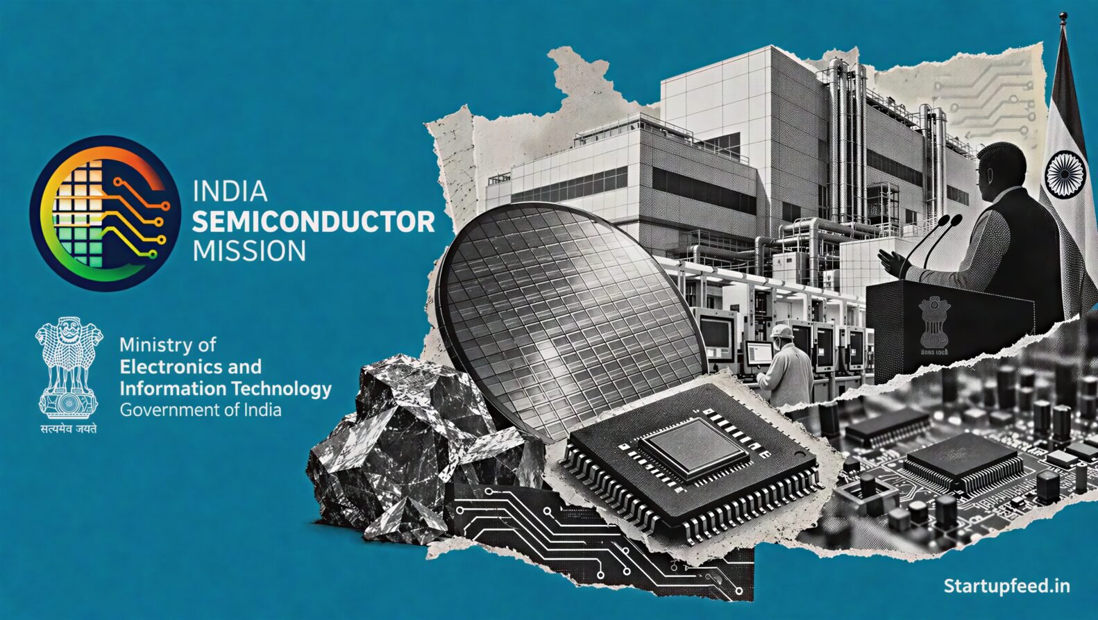
India wants at least 200 deep-tech chip design companies under Semicon 2.0, its next semiconductor phase. Union Minister Ashwini Vaishnaw set that target on September 18, 2026.
He was speaking at a fireside chat during SEMICON India 2026. Vaishnaw holds the Electronics and Information Technology portfolio. His plan puts small design startups and MSME makers at the centre of the chip push.
The base is already there. Under Semicon 1.0, more than 105 startups became chip designers. Of those, 20 raised venture capital worth close to Rs 800 crore, according to earlier government disclosures.
The 200 figure nearly doubles that design cohort. Vaishnaw called it a possible game changer for India’s intellectual property base.
Semicon 2.0 was approved with an outlay of Rs 1,27,500 crore. The first phase ran on Rs 76,000 crore. StartupFeed reported the scheme notification on August 31, 2026.
What is the 200 chip design startup target?
The target is to build at least 200 deep-tech chip design companies under Semicon 2.0. Vaishnaw named this figure at SEMICON India 2026 on September 18, 2026.
Chip design has been the most startup-heavy part of India’s semiconductor plan. The first phase produced over 105 chip design startups from a near standing start.
MSMEs, or micro, small and medium enterprises, sit alongside those designers in the plan. Vaishnaw framed both groups as the backbone of the ecosystem.
Semicon 2.0 rests on six pillars. These are design, materials and machines, more fabs, more assembly and test capacity, research, and talent.
Why did shared software access matter more than cash?
Shared software access did more than direct grants to seed India’s chip design startups. That was Vaishnaw’s own reading of the first phase.
The biggest barrier for young design firms was the cost of design software. These are called electronic design automation, or EDA, tools. Vendors include Cadence, Synopsys and Siemens.
A single EDA licence can cost more than an early startup’s whole yearly budget. So the government did not fund individual licences.



Instead it routed shared access through the Centre for Development of Advanced Computing, known as C-DAC. That let founders design chips without paying the full cost alone.
The barrier to simply trying a chip design fell. More than 105 startups became chip designers as a result. The open question is whether the model holds for a cohort nearly twice the size.
How do MSMEs fit the chip plan?
MSMEs supply the precision parts that the chip and electronics push now needs. Vaishnaw put them at the heart of the manufacturing story.
He cited one executive met at the event, without naming the company. That firm had begun exporting components worth around Rs 2,000 crore from India.
Close to 90% of that component base was sourced from MSMEs. The same precision skills now feed several sectors.
Those sectors include mobile phone making, aerospace parts for firms such as Airbus, and defence. One chief executive said his board had set effectively no cap on India investment, as long as execution kept pace.
| Measure | Semicon 1.0 | Semicon 2.0 |
|---|---|---|
| Outlay | Rs 76,000 crore | Rs 1,27,500 crore |
| Chip design companies | 105 plus | 200 target |
| Design startups that raised VC | 20 | Not stated |
| VC raised by that group | About Rs 800 crore | Not stated |
What is the skilling plan under Semicon 2.0?
The government is rolling out a multi-level skilling plan for the sector. It starts with a 240-hour Level 1 course.
That course is meant to take a student out of high school toward graduate-level skills over successive levels. A Precision Manufacturing Institute is set to launch soon, with more to follow.
On design talent, India set out to train 85,000 semiconductor design engineers over ten years. Around 70,000 were trained within the first four years, a figure Vaishnaw cited in this conversation.
Other recent government statements have put the cumulative total at the full 85,000 target. The exact current count appears to vary by when it was last updated.
The clean room technician target is one lakh under Semicon 2.0. Vaishnaw said this will likely need to be revised upward, given industry demand.
India’s first fab is the Tata Electronics and PSMC plant at Dholera. It is on track for its first wafer in 2028.
What this means for you: If you run or back a fabless chip startup, the design route under Semicon 2.0 is the clearest state-backed opening, so line up your C-DAC tool access and funding case now.
StartupFeed Insight
The number that matters is not 200. It is the jump from 105 to 200 built on shared software, not cash. Semicon 1.0 seeded a design base for a Rs 1,000 crore design outlay, and 20 of those firms pulled in close to Rs 800 crore of private money. That is real leverage. The risk is scale. A shared tool pool that worked for 105 founders may strain at 200, and the government has not said how C-DAC capacity grows to match. Watch the next six months for a hard capacity number. Expect the first Semicon 2.0 design approvals before March 2026.
— Avinash Mishra, Business Correspondent
Frequently Asked Questions
Have a tip? Write to us at editorial@startupfeed.in.
Liked this story? Follow StartupFeed on Google so our reporting reaches you first.