
Quick Take
- Odisha signed a $3.3 Bn (Rs 27,390 Cr) MoU with Intel and 3DGS for India’s first glass-core substrate facility.
- The facility at Bhubaneswar-Khurda will create 1,800 direct high-skill jobs over five to six years.
- Intel joins as technology partner; production is targeted to begin by August 2028, with full scale by 2030.
In This Article
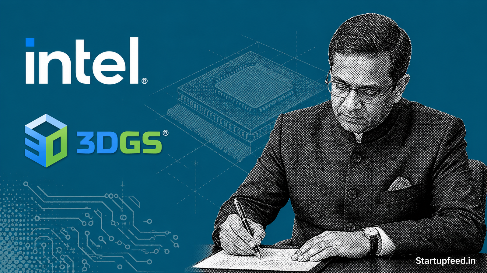
Intel and 3DGS have signed the Odisha MoU for a $3.3 Bn (Rs 27,390 Cr) advanced packaging glass-core substrate manufacturing facility in the Bhubaneswar-Khurda region of Odisha, according to Business Standard’s official report on May 29, 2026.
The agreement was signed on May 28 and 29, 2026, and witnessed by Union Minister of Electronics and IT Ashwini Vaishnaw and Odisha Chief Minister Mohan Charan Majhi. Intel CEO Lip-Bu Tan and 3DGS CEO Babu Mandava also participated, underscoring the strategic weight of this deal for India’s semiconductor ambitions. The facility will be set up through 3DGS’s wholly owned Indian subsidiary, Heterogeneous Integration Packaging Solutions Pvt Ltd (HIPSPL), at Info Valley in the Khurda district.
StartupFeed Insight
The numbers hide the real story. The earlier 3DGS project, approved under the India Semiconductor Mission (ISM) in August 2025, carried a Rs 1,943 Cr price tag. This new MoU puts the combined commitment at $3.3 Bn, roughly 14 times larger. That escalation signals Intel is treating India not as a pilot market but as a long-term packaging hub. Founders building in AI hardware, defence electronics, or 5G components should watch Odisha closely. The ecosystem Intel and 3DGS build around this facility will create supplier and integration opportunities that do not exist anywhere else in India today. Expect the first wave of ancillary semiconductor supplier deals from Odisha by Q2 FY28. By StartupFeed Desk.
What Is the Intel 3DGS Odisha MoU About?
The MoU covers the establishment of an Advanced Packaging Substrate Manufacturing Facility in Odisha. It builds on 3DGS’s existing footprint: the company had already received Union Cabinet approval in August 2025 for a vertically integrated advanced packaging and embedded glass substrate ATMP (Assembly, Test, Marking, and Packaging) facility in the same Info Valley location.
Under the new MoU, Intel steps in as the technology partner. Intel will provide process expertise, technology licensing, quality systems, and workforce capability-building support. The project is expected to come up over five to six years. It will focus on three product lines: advanced packaging glass-core substrates, HDI (High-Density Interconnect) substrates, and associated semiconductor technologies.
The signing was witnessed virtually by Union Minister Ashwini Vaishnaw, who said the project aligns with the government’s vision to develop a complete semiconductor manufacturing ecosystem in India. Odisha Chief Minister Mohan Charan Majhi attended in person. Intel Foundry’s Executive Vice President and General Manager Naga Chandrasekaran said the collaboration will help explore a new opportunity in Odisha and accelerate commercialisation of next-generation advanced packaging solutions globally.

Deal Breakdown: Numbers and Key Players
| Metric | Detail | Notes |
|---|---|---|
| Total MoU Value | $3.3 Bn (approx Rs 27,390 Cr) | Signed May 28-29, 2026 |
| Technology Partner | Intel (process expertise, licensing, QS) | Intel CEO Lip-Bu Tan participated |
| Project Implementer | 3DGS via HIPSPL (Indian subsidiary) | Greenfield facility, Info Valley, Khurda |
| Prior ISM-Approved Investment | Rs 1,943.53 Cr (Central + State support) | Approved August 2025 |
| Direct Jobs Created | 1,800 high-skill positions | Focus on advanced packaging roles |
| Production Target | Commercial output by August 2028, full scale by 2030 | Site engineering already underway |
The most important detail in the table: the $3.3 Bn MoU dwarfs the previously approved Rs 1,943 Cr ISM project. This new commitment signals a scale-up well beyond the original glass substrate pilot.
About 3D Glass Solutions (3DGS)
3D Glass Solutions Inc. (3DGS) is a US-based semiconductor company headquartered in Albuquerque, New Mexico. It develops proprietary glass-ceramic packaging technology based on its APEX platform, which holds over 100 patents. Founded to commercialise RF, photonic, and data centre glass substrate solutions, 3DGS counts Intel Capital, Lockheed Martin Ventures, and Applied Ventures among its investors. In India, it operates through HIPSPL, its wholly owned subsidiary based in Odisha.
Why Glass Substrates Matter for India
A glass-core substrate is a key component in advanced semiconductor packaging. It replaces traditional organic substrates (which use plastic or resin layers) with a glass base. Glass offers lower electrical signal loss, better thermal stability, and the ability to pack more components into a smaller space. This makes it essential for high-performance applications: AI accelerators, 5G base stations, aerospace radar, and data centre chips.
Until the groundbreaking in April 2026, India had no facility capable of manufacturing glass substrates at a commercial scale. Every chip requiring advanced packaging had to be sent abroad, mostly to Taiwan, South Korea, or Japan. The 3DGS facility at Info Valley in Odisha changes that. It is designed to process both internally manufactured glass substrates and externally sourced organic substrates in its initial phase, with a gradual shift toward fully glass-based packaging as the local ecosystem matures.
The facility will serve sectors that Indian startups and corporates are actively building in: AI computing hardware, defence electronics, automotive radar, and 5G or 6G communication systems. It also feeds directly into the India Semiconductor Mission (ISM), the government’s Rs 76,000 Cr program to build a domestic semiconductor supply chain.
How Does This Compare to Other Semiconductor Bets?
India’s semiconductor pipeline has grown fast. The table below shows how the 3DGS-Intel Odisha deal compares to the other major approved projects under the India Semiconductor Mission:
| Project | Investment | Focus |
|---|---|---|
| 3DGS + Intel, Odisha (new MoU) | $3.3 Bn | Glass-core advanced packaging |
| Tata Electronics + PSMC, Dholera | Rs 91,000 Cr | Silicon wafer fab (28nm to 110nm) |
| Micron Technology, Sanand | Rs 22,516 Cr | OSAT (memory chip packaging) |
| HCL-Foxconn, Jewar UP | Rs 3,706 Cr | 20,000 wafers/month chip fab |
What makes the 3DGS-Intel bet different is its focus on glass-core substrates specifically. No other approved Indian project targets this segment. Glass substrates sit at the cutting edge of semiconductor packaging and are still being commercialised globally. India is entering this market at the same time as the US, Japan, and South Korea, not a decade later.


Also Read
- AI and Deep-Tech: Latest Coverage on StartupFeed
- For Founders: What India’s Semiconductor Push Means for Deep-Tech Startups
- Funding and Deals: Track Deep-Tech Rounds in India
What’s Next
Watch for the first formal supplier ecosystem announcements from Intel and 3DGS by Q4 2026. The environmental clearance, SEZ permit, and building approvals for the Info Valley site were already in progress as of April 2026. Commercial production at the initial facility is targeted for August 2028. Will Odisha become India’s first genuine semiconductor manufacturing hub?
Frequently Asked Questions
What is the Intel 3DGS Odisha MoU and how much is it worth?
The Intel 3DGS Odisha MoU is a Memorandum of Understanding signed on May 28 and 29, 2026 between the Odisha government, Intel, and 3D Glass Solutions (3DGS) to set up a $3.3 Bn (approximately Rs 27,390 Cr) advanced packaging glass-core substrate manufacturing facility in the Bhubaneswar-Khurda region. Intel serves as the technology partner, providing process expertise and technology licensing.
What does 3D Glass Solutions (3DGS) do and why is it important for India?
3DGS is a US-based semiconductor company that manufactures glass-ceramic substrate packaging components using its proprietary APEX platform. Glass substrates enable higher chip density, lower signal loss, and better thermal performance than traditional organic substrates. The Odisha facility will be India’s first commercial glass-core substrate plant, serving AI, defence, 5G, and automotive chip sectors.
When will the Odisha semiconductor facility start production?
The Intel 3DGS Odisha MoU project is expected to take five to six years to fully complete. 3DGS’s Indian subsidiary HIPSPL has already completed soil testing and preliminary engineering at Info Valley in Khurda. Commercial production is targeted for August 2028, with full-scale output by August 2030.
Liked this story? Follow StartupFeed on Google so our reporting reaches you first.